Researchers globally are striving to enhance qubits, the tiny fundamental units of quantum computers. These qubits are extremely delicate, making them prone to errors that can reduce the efficiency of the devices. A new cluster tool at MIT.nano is set to empower scientists to further improve qubit performance.
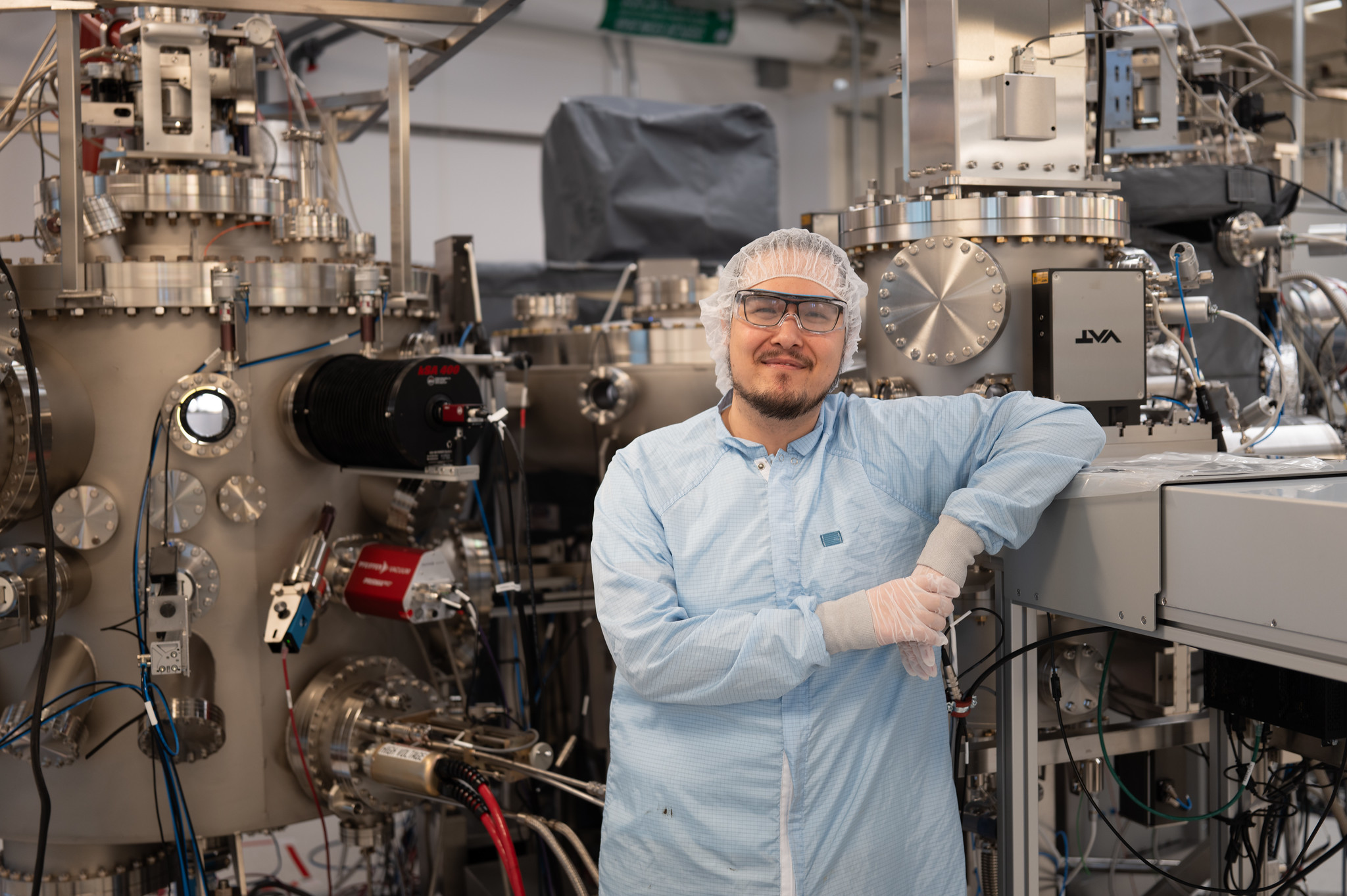
Recently, people passing by MIT.nano may have noticed the installation of intricate equipment on the cleanroom’s first floor. This state-of-the-art apparatus is a custom-built molecular beam epitaxy (MBE) system, resembling a sci-fi movie prop. It functions under ultra-high vacuum to create high-quality thin films, enabling the growth of crystalline materials on wafers. This tool will aid quantum and materials researchers in examining how film growth influences the materials used in qubit production.
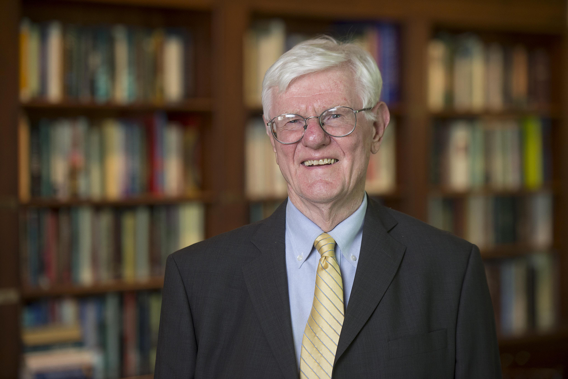
William D. Oliver, a professor at MIT, stated that realizing quantum computing’s potential requires robust and reproducible qubits. While past improvements in superconducting qubit performance were mainly due to circuit design, future advancements must focus on materials science and engineering to minimize environmental noise. The new MBE system is ideal for this purpose, and MIT.nano is the perfect location for such research.
MIT.nano is well-equipped for this system with its physical space, climate controls, and expert staff. Oliver’s Engineering Quantum Systems (EQuS) group can operate the tool in a high-performance environment. The MBE requires a controlled setting, explained by Patrick Strohbeen of the EQuS group, likening it to an inverted International Space Station with a vacuum chamber surrounded by atmosphere. This vacuum, maintained at negative 90 degrees Celsius, allows precise atomic-scale thin film growth.
The MBE system, covering 600 square feet, comprises six chambers. The process begins in the load lock, where wafers are adjusted from atmospheric pressure to near vacuum. The wafers then pass through a distribution center to various chambers, including the deposition chamber for material growth and the oxidation chamber for ceramic material development. A unique feature is the sixth chamber for X-ray photoelectron spectroscopy (XPS), enabling researchers to analyze material structure changes without exposing them to the atmosphere.
Strohbeen emphasized the importance of understanding the materials platform for quantum devices, which has been challenging to study due to buried interfaces. He compared it to determining the amount of ice under snow without disturbing the layers. The XPS chamber allows detailed study of these interfaces without altering their environment, making it a “materials scientist’s playground.”
Oliver, also the director of the MIT Center for Quantum Engineering, chose MIT.nano for the MBE Quantum system due to its 45,000 square feet of cleanroom space and necessary infrastructure. Nick Menounos of MIT.nano highlighted the facility’s stable utilities and lab environment, essential for the MBE system’s purity and repeatability. Early collaboration and foresight in procurement facilitated a swift installation process.
MIT.nano staff played a crucial role in the successful setup of the MBE system, which focuses on improving qubit scalability and yield by minimizing environmental variables. The cleanroom setting also supports new device research with various fabrication tools available. Strohbeen expressed excitement about the tool’s potential for both materials science and device development.
The MBE system was funded by grants from the Army Research Office and the Laboratory for Physical Sciences. This acquisition supports MIT’s strategic initiatives, such as the MIT Quantum Initiative, which seeks to leverage quantum advancements for significant challenges in various sectors.
Original Source: news.mit.edu